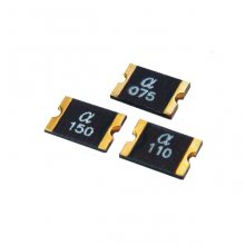
| ��Ʒ���ԣ��Իָ���Ƭ | �ӹ����ƣ��� | Ʒ�ƣ��ش� |
| �ͺţ�1812 | ���ࣺ����˿ | ��;������ |
| ������� | ��ѹ���ԣ���ѹ | ��״����Ƭʽ |
| �۶��ٶȣ�F/���� | ִ�б������� | �Զ���λ���ܣ��� |
| ����ѹ��32V | ��������3A | �¿ط�Χ��- 40 ��C ��85 ��C�� |
Performance Specification :
Features:
•Surface Mount Devices •Lead free device
•Surface Mount packaging for automated assembly •Agency recognition: UL
Applications:
Almost anywhere there is a low voltage power supply, up to 60V and a load to be protected,including:
■ Computer mother board, Modem. USB hub
■ PDAs & Charger, Analog & digital line card
■ Digital cameras, Disk drivers, CD-ROMs

Ihold= Hold Current. Maximum current device will not trip in 25°C still air.
Itrip= Trip Current. Minimum current at which the device will always trip in 25°C still air.
Vmax= Maximum operating voltage device can withstand without damage at rated current (Imax).
Imax= Maximum fault current device can withstand without damage at rated voltage (Vmax).
Pd= Maximum power dissipation when device is in the tripped state in 25°C still air environment at rated voltage.
Rimin/max= Minimum/Maximum device resistance prior to tripping at 25°C.
R1max= Maximum device resistance is measured one hour post reflow.
CAUTION : Operation beyond the specified ratings may result in damage and possible arcing and flame.
Environmental Specifications:
Ambient operating conditions : - 40 °C to 85 °C
Maximum surface temperature of the device in the tripped state is 125 °C
AGENCY APPROVALS :
U.L approved
Ihold versus temperature
I hold versus temperature:
Construction and Dimension (Unit:mm):
Termination pad characteristics
Terminal pad materials: Tin-Plated Nickle-Copper or Gold-Plated Nickle-Copper
Terminal pad solderability: Meets EIA specification RS186-9E and ANSI/J-STD-002 Category 3.
Rework
Use standard industry practices, the removal device must be replaced with a fresh one.
Thermal derating curve:
WARNING:
· Use PPTC beyond the maximum ratings or improper use may result in device damage and possible electrical arcing and flame.
· PPTC are intended for protection against occasional over current or over temperature fault conditions and should not be used
when repeatedfault conditions or prolonged trip events are anticipated.
· Device performance can be impacted negatively if devices are handled in a manner inconsistent with recommended electronic,
thermal, andmechanical procedures for electronic components.
· Use PPTC with a large inductance in circuit will generate a circuit voltage (L di/dt) above the rated voltage of the PPTC.
· Avoid impact PPTC device its thermal expansion like placed under pressure or installed in limited space.
· Contamination of the PPTC material with certain silicon based oils or some aggressive solvents can adversely impact the
performance of thedevices. PPTC SMD can be cleaned by standard methods.
· Requests that customers comply with our recommended solder pad layouts and recommended reflow profile. Improper
board layouts orreflow profile could negatively impact solderability performance of our devices.
‧Recommended reflow methods:IR, vapor phase oven, hot air oven.
‧Devices are not designed to be wave
soldered to the bottom sideof the board.
‧Recommended maximum paste thickness is
0.25 mm (0.010 inch).
‧Devices can be cleaned using standard
method and solvents.
Note:If reflow temperatures exceed the recommended
profile,devices may not meet the performance
requirements.
Tape And Reel Specifications (mm):
��ݸ���ش��������˾ �ֻ���𐀄𐀅𐀅𐀆𐀇𐀈𐀉𐀄𐀊𐀋𐀉 �绰��𐀋𐀇𐀍𐀎𐀉𐀍𐀊𐀆𐀉𐀉𐀅𐀉 ��ַ���㶫 ��ݸ ʯ���� ��ݸ��ʯ�������ϴ�������·43��